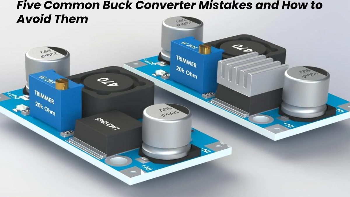
The Buck Converter is used in SMPS circuits where the DC output voltage needs to be lower than the DC input voltage. It functions by taking an input directly from a DC source, such as a battery, lowers or ‘bucks’ the input voltage of an unregulated DC supply and converts it to a lower stabilised output voltage.
The buck connector converts the DC whether obtained from mains supply or a transformer, to a high frequency AC. This is done via a switching or ‘chopper’ transistor which can be driven by a square wave. The resulting high frequency AC wave is efficiently re-converted to DC by the buck converter. Buck converters have very high efficiencies, often exceeding 95%.
Though buck converters are highly effective, there are several common mistakes in their design which should be avoided to ensure best performance.
Table of Contents
1. Insufficient input and output decoupling capacitance
Mistakes in the selection of the capacitor can cause oscillations which may be incorrectly interpreted as low phase margin in the control loop. To avoid incorrect inferences being drawn the input supply to the converter must either be properly bypassed with input capacitance, or long bench power supply leads used. Perturbations can be avoided by connecting the input of the EVM to a bulk input to a decoupling capacitor.
Insufficient input decoupling can also cause the input voltage to dip below the input undervoltage lockout (UVLO) level which will result in turning the converter off.
2. Minimum On-Time Violation
Selecting the incorrect switching frequency (fSW) can cause ripples in the voltage output for a buck converter in normal operation. The ripple is caused because of violations of the
minimum on-time of the buck converter IC. To avoid this potential problem, select the switching frequency by considering the maximum input voltage and maximum minimum on-time as listed in the product datasheet. As the minimum on-time can vary according to output current and temperature, the maximum minimum on-time value should be used.
3. Thermal Derating
The operating temperature of a part should be as low as possible for optimal performance of the buck converter. If a part is forced to operate over its rated junction temperature a thermal shutdown may result. This may also reduce the longevity of the part. To ensure ideal thermal performance you should consider the effective average load current. Be aware that variations in the PCB layout my also impact thermal performance.
4. Poor Control Loop Compensation
After the selection of key power components, the control loop must be properly compensated. Insufficient slope compensation can lead to subharmonic oscillations appearing when the peak current mode control converter is at under 50% duty cycle. To ensure that the gain margin is sufficient design goal recommendations are a minimum phase margin of 45° and gain margin of -10 dB.
Taking variations across operating conditions and between components into consideration, the margin of a nominal circuit should be higher so minimum values are met.
Following these simple guidelines can ensure that your buck converter performs at its most efficient level. Consult your supplier for the best buck converters available.